As the demand for higher performance and power efficiency in semiconductor devices intensifies, advanced packaging techniques like 2.5D and 3D Cu-to-Cu hybrid bonding are becoming increasingly critical. However, these technologies present complex manufacturing challenges, particularly in material selection and process innovation.
2.5D Interposer Materials
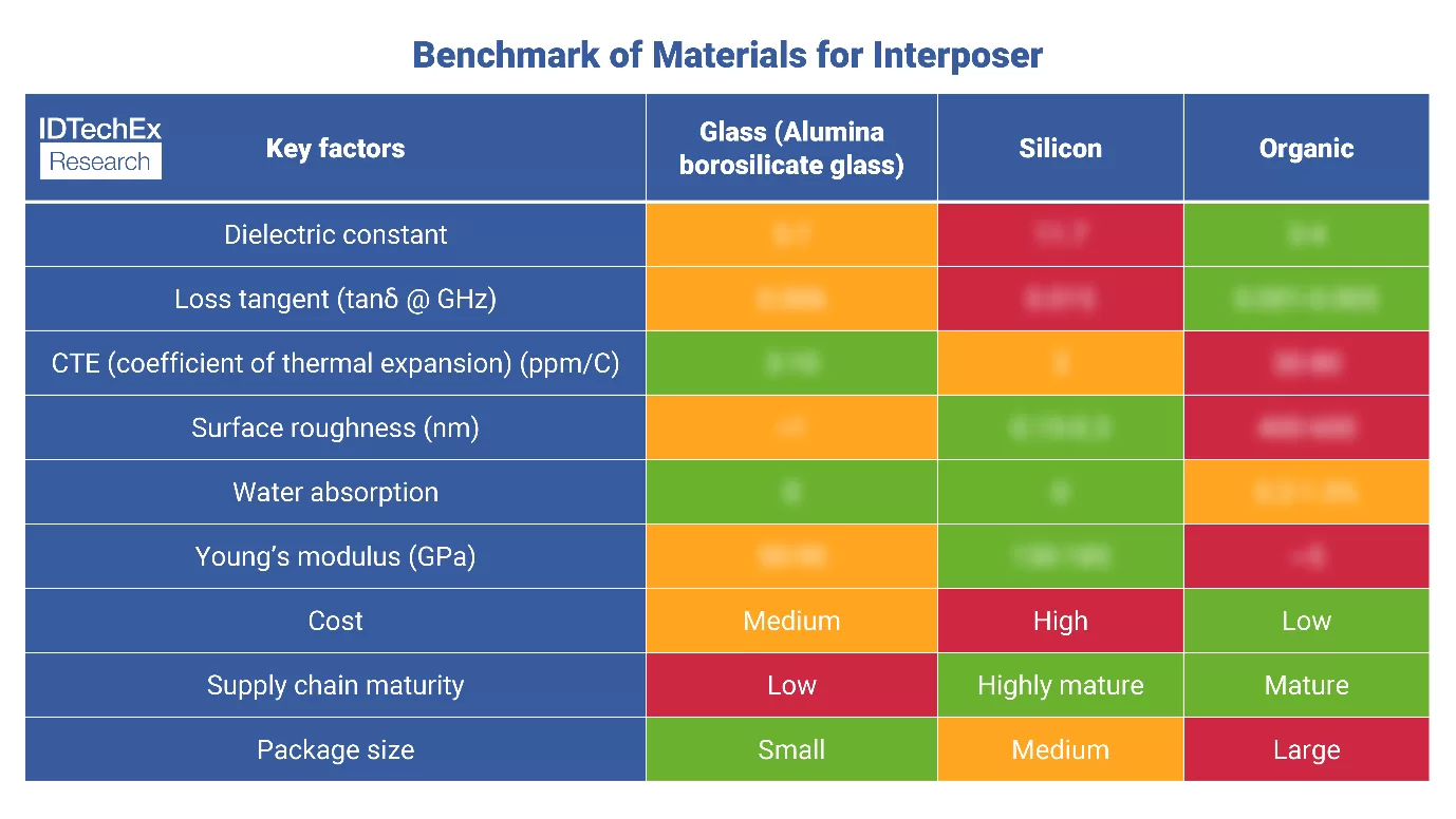
2.5D packaging utilizes interposers to horizontally interconnect different chiplets. Three primary materials are used for interposers: silicon (Si), organic, and glass. Silicon interposers are the industry standard for high-performance computing (HPC) due to their ability to support fine routing, but their high cost and limited packaging area pose challenges. Localized Si bridges are emerging as a potential solution.
Organic interposers offer a cost-effective alternative, particularly through Fan-Out Panel Level Packaging (FOPLP), which increases area utilization and lowers costs. However, achieving fine routing comparable to silicon remains a challenge.
Glass interposers, with their tunable coefficient of thermal expansion (CTE) and high dimensional stability, also support panel-level packaging and cost reduction. However, the production of glass interposers is still maturing, limiting widespread adoption.
Key Material Selection Criteria
Selecting materials for interposers in 2.5D packaging involves considering five key criteria: dielectric constant (Dk), elongation to failure, CTE, Young’s modulus, and moisture absorption. Balancing these parameters is crucial for optimizing performance and reliability.
Cu-Cu Hybrid Bonding Manufacturing
Wafer-to-Wafer (W2W) and Die-to-Wafer (D2W) hybrid bonding are two primary approaches for 3D hybrid bonding. W2W bonding is a more established process that involves bonding two full wafers, offering high throughput and consistency. However, it lacks flexibility in handling different chip sizes.
D2W hybrid bonding provides greater flexibility by bonding individual dies onto a target wafer, enabling the integration of various die sizes and types. However, D2W presents challenges in terms of surface cleanliness, alignment precision, and die aspect ratios.
IDTechEx Report
The “Materials and Processing for Advanced Semiconductor Packaging 2025-2035: Technologies, Players, Forecasts” report by IDTechEx provides in-depth insights into the material and processing trends in advanced semiconductor packaging. The report covers 2.5D and 3D packaging technologies, market forecasts, and player analysis.
About IDTechEx
IDTechEx provides trusted independent research on emerging technologies and their markets. Since 1999, we have been helping our clients to understand new technologies, their supply chains, market requirements, opportunities and forecasts. For more information, contact research@IDTechEx.com or visit www.IDTechEx.com.